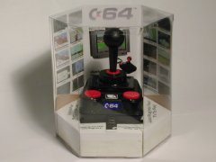
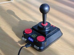
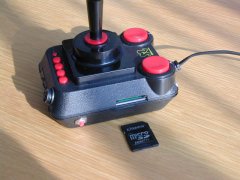
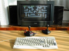
C64 - DTV2 with keyboard, joysticks and a 1541-III
Introduction
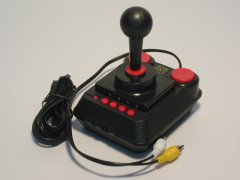 This article is about hacking a C64 DTV-2 (PAL version). The following will be added: 1541-III, keyboard, external power-supply and two joysticks.
This hack is not simple but can be done with some basic tools:
- Mini drilling machine like a Dremel.
- Some drills an cutters.
- A couple of needle files, screwdrivers.
- Small pliers, mini saw, etc.
- Soldering iron for electronics (Weller WECP-20)
- Multi-meter with V, A, Ohm, "beep"
Related links.
The 1541-III.
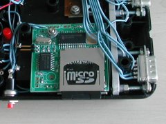 This is a modern version of an original 1541 Commodore disk drive. The 1541-III is based on a micro controller that is connected between the CBM serial bus and a SD memory card. With some commands you can attach a D64 file on the SD card to the serial bus. This means that for example a C64 or a DTV will think that a real 1541 disk drive is connected. The pro's are that the 1541-III is very small and can hold up to 512 diskettes on the SD memory card (8.3 format). The con's are that the 1541-III is not a perfect copy, so some programs will not work.
Firmware: Inside the micro controller there is software this is called firmware. This firmware will tell the micro controller how to do its work. The firmware for the standard 1541-III and the DTV version of the DTV-III is the same. This firmware is developed by Jan Derogee.
The 1541-III was developed by Jan Derogee. This version can be connected as a external device to a C64 or a DTV. Powersupply for this version is 5 volts DC.
The 1541-III DTV version was developed by Pyrofer and Jussi Saily. Because this version is much smaller it can be build inside of a DTV. Power supply for this version is 3,3 volts DC.
The parts.
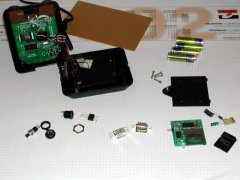 You will need some components:
- 1 x 1541 III, DTV version
- 2 x DB9 male connectors (Joystick)
- 1 x PS/2 female connector (Keyboard)
- 1 x Voltage plug 2,1 mm
- 1 x Push button switch "make"
- 1 x Experimental PCB (30 x 40 mm)
- 1 x Voltage regulator 5 VDC (positive) e.g. 7805, 1 Amp
- 1 x 22 uF capacitor
- 1 x 100 nF capacitor
- 1 x Diode 1N4007
- some nuts and bolts to attach everything.
- lots of wire (flat-cable)
First get the connectors en the electronic parts. You can buy them at a local electronics shop.
Before cutting the holes the plastic box make sure the connectors and electronics have enough space when the DTV is closed.
Here you can see the start of the project.
The DTV is opened and all the parts are collected. On the right you can see the 1541-III. Also the reset switch for the 1541-III, two joystick connectors, keyboard connector and a voltage input connector.
This DTV will run on batteries and a mains adapter.
Test fitting the parts.
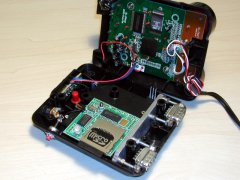 On the photo you can see that the main components are installed. Also the housing is cut at several places.
The joystick connectors are mounted on a piece of aluminum for extra strength.
Top middle of the photo you can see the back-side of the PS/2 keyboard connector. On the left the voltage input connector and the reset switch for the 1541-III. On this photo you can see capacitor C5. This is sticking out to far and will hit the holder of the SD card. This capacitor has to be moved.
Joystick connector support.
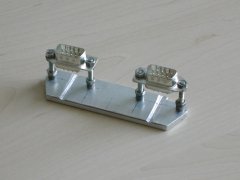 This is the construction that holds the joystick connectors. The aluminum plate is placed between the battery holder and the two pillars that support the fire buttons.
The plate is made to fit exactly inside the DTV.
The position of the connectors is adjusted with the bolts and nuts. When the position is correct the bolts are shortened.
Altering the on / off switch.
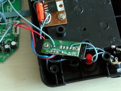 This DTV will work on both batteries and a mains adapter. For this to work the on / off switch is modified. The not used contact of the switch is used by disconnecting it from the circuit board. A copper line is cut. See photo. On this connection I attached the +5 Volt from the power supply (mains adapter). If the DTV is "ON" it will work on batteries and if it is switched "OFF" it will run on a mains adapter. To prevent troubles with the electronics of a external keyboard it will only be connected when the 5 volt power supply via the mains adapter is selected. On batteries you can still use the virtual keyboard.
Connecting the wires.
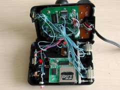
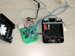 You can see that all wires are connected on the DTV PCB. I labeled all the wires to make the connections at the other end more easy.
If you use thin wire you can put the wire in the little holes in the PCB and solder them.
I used (IDE) cable from an old PC.
It maybe necessary to remove the green protective coating from the PCB where you need to solder.
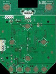
The PCB (bottom).
The PCB (top).
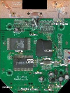 The connections below are described as in the pictures of the PCBs. The TPx numbers are on the picture of the bottom side of the PCB. The Rxx Numbers are on the top side of the PCB. (Top side is where the chips are) The yellow dots are the soldering points for the extra connections.
The joystick on the DTV is: JOYA
JOYA UP = Joystick Port 2 Up
JOYA DN = Joystick Port 2 Down
JOYA LT = Joystick Port 2 Left
JOYA RT = Joystick Port 2 Right
JOYA FE = Joystick Port 2 Fire
JOYB UP = Joystick Port 1 Up
JOYB DN = Joystick Port 1 Down
JOYB LT = Joystick Port 1 Left
JOYB RT = Joystick Port 1 Right
JOYB FE = Joystick Port 1 Fire
IEC ATN = Disk-drive IEC ATN (TP1 - The hole just right of R13)
IEC CLK = Disk-drive IEC CLOCK (TP8 - The hole just below the left side of R35)
IEC DTA = Disk-drive IEC DATA (TP9 - The hole just below the left side of R47)
KEYB DTA = Keyboard DATA (TP4 - The hole just above of R4)
KEYB CLK = Keyboard CLOCK (TP3 - The hole just above of R3)
+ 3,3 VDC = power supply for the 1541-III - The hole between R3 and R4.
+ 5 VDC from the voltage regulator is connected to the + of the battery holder.
GND from the voltage regulator is connected to the a extra connection on the modified on / off switch. On this little PCB you have to cut a copper line. See photos above.
The schematic.
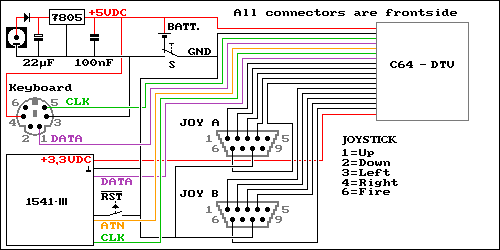 This is the schematic I used inside the DTV.
In the top left corner of the schematic you see the 5VDC power supply. The diode prevents wrong polarity of the mains adapter. The mains adapter has to be a direct current version with about 9 VDC output. The voltage is transformed into a ripple free DC voltage by the capacitor (22 uF). Next the 7805 voltage regulator will change the voltage to exactly 5 VDC. The capacitor (100nF) will filter out any interference.
Below the power supply the keyboard connector is drawn. Because of the limited space I have chosen for a PS/2 connector. The keyboard is fed with 5 VDC and GND (only when its running on a mains adapter). The clock signal and the data signal are connected to the DTV2 unit.
In the bottom left corner you can see 1541-III. The connections are +3,3VDC from the DTV, GND ,data, atn and clock. An extra switch is connected so you can reset the 1541-III without resetting the DTV2 unit.
In the middle there are two joystick ports. The joystick signals are connected to the DTV2 unit.
All the wires that go to the DTV2 unit are marked in one of the photos.
Checking
Closing the DTV.
The end result.
Testing the C64 - DTV
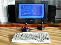 Connect your keyboard and mains adapter.
Turn on the DTV2 unit. The DTV2 should boot normally like nothing has changed.
After it has booted press down on the "CTRL" on your keyboard. Reset the DTV2 while holding down the "CTRL" on your keyboard. If you get the C64 blue start screen let go of the "CTRL" key. To be quicker at boot up do the RESET and "CTRL" straight after turning on the power.
Loading a game.
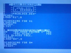 LOAD"$CARD",8 [ENTER]
LIST [ENTER]
LOAD"$1",8 [ENTER]
LIST [ENTER]
LOAD"PAC-BOULDER",8 [ENTER]
RUN [ENTER]
With LOAD"$1",8 the D64 is selected. In this example it is the 1st D64 in the list.
With LOAD"PAC-BOULDER",8 you load the game. "PAC-BOULDER" is just an example.
Go and use it to play all those great games............
The use of the external joystick ports.
Update:
 The DTV functioned a couple of days without problems. But after a while it went wrong with loading from the 1541-III DTV. And after a while it gave the error: FILE NOT FOUND ERROR at every attempt at loading.
The DTV was present at one of the meetings of the Dutch Commodore User Group. After a few checks the problem was not found. But Jan Derogee saved the day. After a short check he discovered the fault. The switches of the SD card holder were not alright.
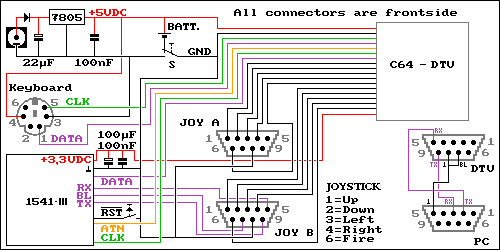
The DTV is now changed with the following items. The switches of the SD card are now always "on". (This is the same as the older version of the 1541-III DTV.) Also Jussi Saily and Jan Derogee advised to add two capacitors to the power supply of the 1541-III DTV. This will stop interference signals.
The firmware cable.
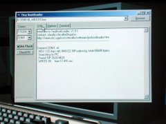
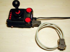 The next question was how do you update the firmware in the 1541-III DTV? There are only two signals (RX and TX) and a ground needed. I had the idea to use the un-used pins of the joystick connector. Jan Derogee gave me the tip to connect the Boot loader Jumper to the joystick port.
In the updated schematic you can see the connections of the firmware update cable.
The short between 7 and 8 on the DTV side of the cable connects to the boot loader input if the cable is connected.
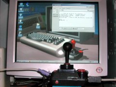
On the photo the DTV with the special cable.
DTV on the PC.
Update: 2019-05-11 13:26:40
